At LiTE Design, we offer a comprehensive range of PCB design services tailored to meet diverse needs. Our expertise spans across various types of PCB designs to ensure that we deliver high-quality and reliable solutions. Here’s an overview of our PCB design capabilities:
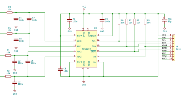
Schematic Design
Component Footprints Design: Accurate design and layout of component footprints to ensure compatibility and performance.
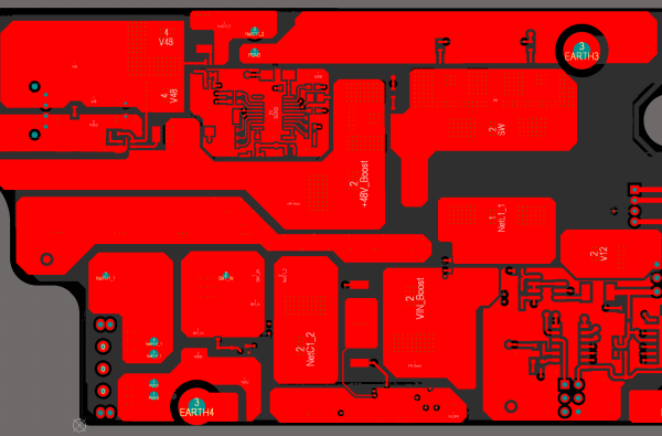
Layout Design and Gerber: Creation of detailed layout designs and Gerber files in RS247X format using industry-standard tools such as Cadence, Orcad, and Allegro.
Zuken Cadstar, Altium Designer: Comprehensive solutions for a wide range of design requirements.
Advanced Analysis
Signal Integrity: Ensuring reliable signal transmission with thorough analysis and optimization.
Thermal Analysis: Managing heat dissipation to maintain optimal performance and reliability.
Design Complexity
Single Layer to 64 Layers: Expertise in designing PCB boards ranging from single-layer to highly complex 64-layer multi-layer boards.
FPGA Processor and FLASH Memory: Design of high-complexity PCBs including external peripheral devices, capable of handling up to 64 layers.
Analog, Digital, and Mixed Signal Boards: Design of boards incorporating analog, digital, and mixed signals with appropriate constraints.
Complex Digital Processor Cards: Development of intricate digital processor cards with over 4000 components.
Power and Specialty Designs
Low/High Wattage Power Converter Layouts: Design of power modules with specific wattage requirements.
Rigid and Flexible Dense Board Designs: Creation of both rigid and flexible PCBs with high-density layouts.
Board Design for Test Jigs: Custom designs for various types of test jigs to ensure precise testing and validation.
Design Outputs
At LiTE Design, we ensure that every PCB design project is completed with precision and detail. Our design outputs are crafted to meet all manufacturing and operational requirements. Here’s a comprehensive overview of what we provide:
PCB Layout Board File
Gerber Files: We provide Gerber files in various formats, including .gbx, .gbr, and .spl, as well as RS274X templates, essential for PCB fabrication.
Silk Screen, Drill Drawings, and Solder Mask: Detailed drawings and files for silk screening, drilling, and solder mask application to ensure accurate and effective manufacturing.
Complete Layer Information: Comprehensive details on all layers, including PTH (Plated Through Hole) and NON-PTH (Non-Plated Through Hole) layers.
Verification and Compliance
Netlists: Generation of netlists to verify electrical connections and ensure design accuracy.
DRC Rules Checking: Thorough checking of Design Rule Constraints (DRC) including line width, track-to-via spacing, and component violations. Penalization measures are applied if required to ensure compliance with design standards.
PCB Fabrication
Fabrication Ready Files: Complete and ready-to-use files for PCB fabrication, ensuring a smooth transition from design to manufacturing.